Quick and Dirty Video Sync Combiner
Generally speaking, when I’m putzing around with old retro computer/video game equipment I’m usually using one of my BVMs as a display. These BVMs only support a composite sync. In the last fear years I’ve had to deal with a few computers that out had outputs for separate HSYNC and VSYNC signals, such as the Atari 520 STE. In order to use the BVMs with these machines, I had to build a simple sync combiner circuit. Since this is a pattern I’ve run across a few times, I figured I’d share the basic theory and schematic with you all.
What are sync signals?
First, a little background for the uninitiated. Sync signals are sent from a device, like a computer or video game system, to a display to tell that display where on the screen it should be drawing the content of the video signal. In the case of VSYNC (vertical sync) the signal goes low 50 times a second for PAL or 60 times a second for NTSC. This tells the display that it’s about to receive data for an entirely new frame and it should start scanning from the start. HSYNC is similar, except it tells the display when it should start a new line. For PAL this signal goes low at a frequency of roughly 15.625kHz and NTSC does the same at about 15.734kHz. This is the kind of syncing you’d see on a VGA display, for instance.
Other devices, like video game systems, often output (or have easily available on the board) a single CSYNC that contains both signals on the same wave form. You’ll often find this in devices that either produced SCART-based RGB or entirely composite output.
Our starting point
Here’s the scope output of the HSYNC and VSYNC signals from a PAL Atari 520 STE I’ve been playing around with. The purple channel is the VSYNC, which is going low at 50Hz. The yellow channel is the HSYNC which is going low at a good 15.6kHz
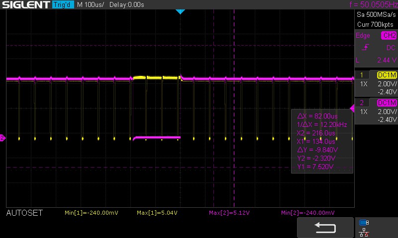
Our task is to combine these into one.
The plan
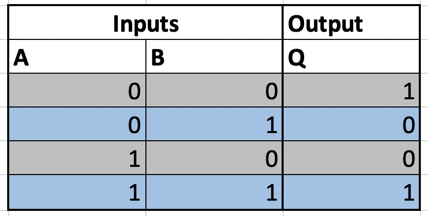
We need to build a circuit that takes two sync inputs and produces a single, composite sync output. What’s important in terms of how the sync signals is interpreted by the display is that we pull the signal low if either of the sync signals are low, and that we keep driving the line high if both are high. This can easily be accomplished with an XNOR gate. Consider the XNOR truth table.
So, in terms of brains, we only need a single XNOR logic gate.
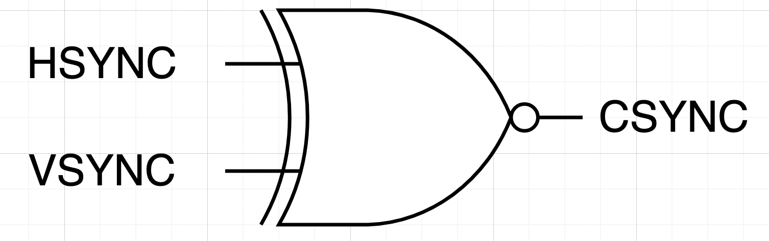
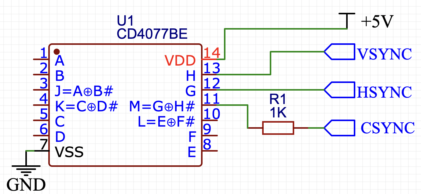
The schematic
Sounds easy enough, but how do translate this to a practical circuit. Well, we can use a CD4077 XNOR gate (U1) to make our lives easy here. Since the output will be at logic levels, we’ll use a 1K resistor to drop the voltage to something the display will be happier with. It might work if you leave it at 5V, but you’ll be over-driving the heck out of the display and things will get hot in a hurry.
After slapping the circuit together on a breadboard, here’s the scoped output of the CSYNC line. See the mostly solid low in the middle where the single more-or-less inverts? That’s the VSYNC being pulled low. The rest of the shorter lows are HSYNC.
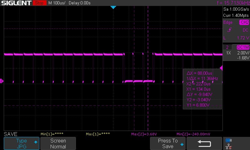
Note that using an XNOR gate like doesn’t result in edge timings that are exactly to spec. It’ll certainly work well enough on most displays, but isn’t perfect. Great for a quick-and-dirty solution, though.
Conclusion
And, that’s it! We have a functioning sync combiner that, when accompanying RGB signals, allows us to display our Atari 520 STE or other device with separate syncs on a BVM.